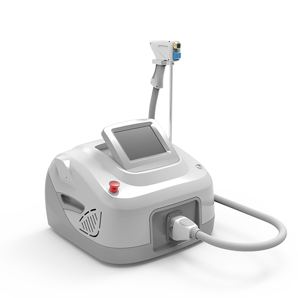
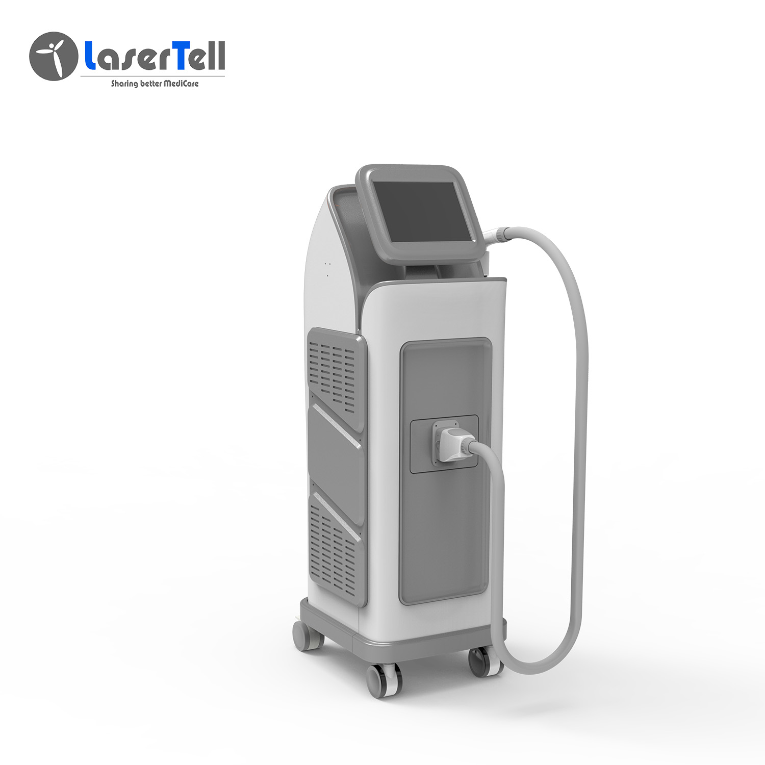
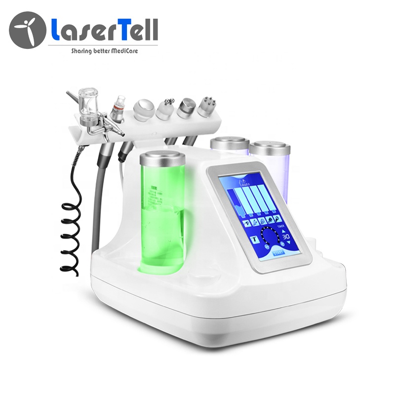
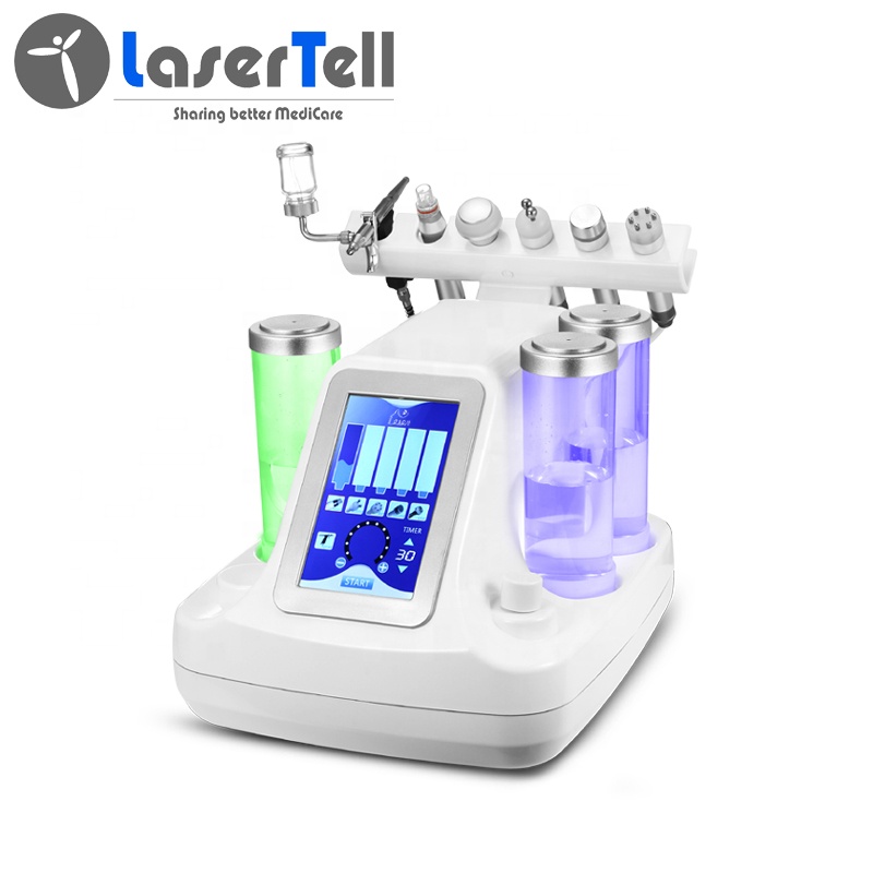
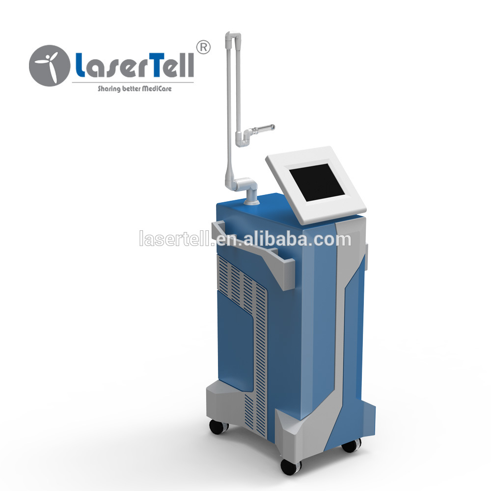
Mini salon spa commercial long lifetime 808nm diode led hair removal laser machine Portable diode laser
What is LED hair removal?

Strength:
1. Bars come from top brand American Coherent;
2. Hard solder AuSn for high stability and reliability;
3. Macro channel cooling structure, easy to use;
4. Square light spot, good energy concentration;
5. Front window plate with anti-reflection film for less power loss;
6. Manufactured in cleanrooms and fully sealed with nitrigen inside for excellent environmental compatibility.

|
Technology
|
|
IPL
|
Diode Laser
|
LED
|
|
Light source features
|
Light source
|
Xenon lamp
|
Diode laser bars
|
LED chips
|
|
wavelength
|
Wide spectrum 610nm-900nm
|
Single wavelength 755/808nm/1064nm
|
Narrow spectrum 780-850nm
|
|
|
Light power
|
5-10kw
|
320-1000w
|
840w
|
|
|
Light emitting area shape
|
Columnar
|
Line
|
Surface
|
|
|
Pulse lifespan
|
10000-30000shots
|
8-30million shots
|
60-100 million shots
|
|
|
Operation
|
Operation mode
|
Stamp
|
Stamp/Repeat
|
Stamp/Repeat
|
|
Energy density
|
1-40j/cm2
|
Stamp:50-100cm2
Repeat:5-12J/cm2@10Hz |
Stamp:50-100cm2
Repeat:5-12J/cm2@10Hz |
|
|
Maintenance
|
Handle
|
Always need change light tube
|
Laser generator is easily damaged, need replace every 1 to 2 years
|
If normal use and regular maintenance, handle has the same lifespan as device
|
|
Filter
|
No need
|
Need often change filter and deionizer, if not, laser generator is easily damaged
|
No need
|
|
|
Cooling water
|
Drinking water
|
Special deionized water or coolant
|
Drinking water
|
Specification
|
Product Name
|
iMED_LED
|
|
Light source
|
LED
|
|
Light spectrum
|
NIR
|
|
Light power
|
800W
|
|
Pulse width
|
10-300ms
|
|
Energy density
|
1-100J/cm2
|
|
Frequency
|
1-10Hz
|
|
Skin type
|
I-VI
|
|
Operation mode
|
Stamp, Repeat
|
|
Spot size
|
15*15mm2
|
|
Cooling system
|
TEC Sapphire contact cooling/ Water cooling
|
|
Cooling temperature
|
15℃ – 10℃
|
|
Size
|
50*46*35cm
|
|
Net weight
|
25KG
|
LED hair removal technology
LED hair removal use high-power super-emitting LED (Planar LED) array (12 pieces of chip) as a light source, crystal guide pyramid shaping and transmission of NIR beam, act on the subcutaneous, melanin in hair follicle absorb heat, to achieve hair removal effect.


Long lifespan and high stability
Up to 100 million shots and 5 years’ expected service lifetime(less than 10% failure and 20% power attenuation), without any consumable. Stable performance, low malfunction rate, no downtime. Very easy maintenance and after sales services. Low running cost, but high return on investment.
Reasonable light wavelength and spectrum
iMED LED use near infrared light with wavelength 780~850nm, little absorbed by skin tissue and vascular etc., but mainly absorbed by melanin in follicle, so hair removal is highly effective. Light spectrum has width, so can apply to more skin colors including dark skin.
Reasonable light wavelength and spectrum
A Evenly rectangle spot with nice consistency, energy is uniform, no painful feeling during treatment. Surface array light source,lower max. local brightness, no harmful to human eyes though direct watch. B Planar light emitting area, uniform rectangular spot,and the light’s divergence angle is small to 15°, easily penetrate into skin, very deep penetration depth, deep hair follicle also can be treated.
|
|
Diode laser
|
LED
|
LED Advantages
|
|
Thermal damage
|
Light power
|
Similar
|
|
|
Thermal power
|
Similar
|
||
|
Chip size
|
1*10mm
|
7.5*7.5mm
|
|
|
Conclusion
|
Similar total thermal power, LED has bigger heat dissipation are and smaller heat flow density.
|
||
|
Heat transfer patch
|
Pass to the bottom and rear Average path is 1.5mm
|
Pass to the bottom Average path is just 0.2mm
|
|
|
Conclusion
|
LED has very short heat transfer path, lower thermal resistance and much higher efficiency of heat dissipation.
|
||
|
Mechanical damage
|
Stress
|
Rectangle, high length-width ratio. Under stress of thermal deformation and thermal fatigue, chips easily desoldering or broken in
pulsed working |
Square, 1:1 length-width ratio. Extra thin chip and large soldering area firmly but low stress.
|
|
Conclusion
|
Because of chip structure, LED chip’s stress is smaller than diode laser
|
||
|
Optical damage
|
Light power
|
Similar
|
|
|
Light emitting area
|
Size 0.01*0.1mm High brightness, foreign body pollution can cause light-emitting surface burned
|
Size 5*5mm Brightness is just similar to normal LED lamp of flashlight, slight dust will not being ignited to burn the lighting
surface |
|
|
|
Conclusion
|
Because of surface emitting, the brightness of LED light emitting area is much smaller than diode laser.
|
|
|
Chain damage
|
|
Not like diode laser, for LED chips, single area’s failure does not affect other emitting area
|
|
Before & After


Company Profile


CUSTOMER FEEDBACK

Write your message here and send it to us

